
As multi-rail embedded designs push tighter reset thresholds and faster brown-out detection, designers increasingly choose high-accuracy, separate-sense voltage detectors. This guide compiles the complete electrical specs and pinout for XC6138NAPP6R-G, with practical test steps and integration notes to shorten time-to-market. The overview below summarizes intent and primary reference strategy for hardware and firmware teams validating reset behavior and system reliability.
The goal is a single-source reference for electrical specs, pinout, typical application circuits, test procedures and compatibility tips for XC6138NAPP6R-G. Where numeric values are shown, they are described as representative and should be verified against the official product datasheet before production. This article emphasizes measurable checks and PCB-level best practices for reliable deployment.
1 — Product overview & background
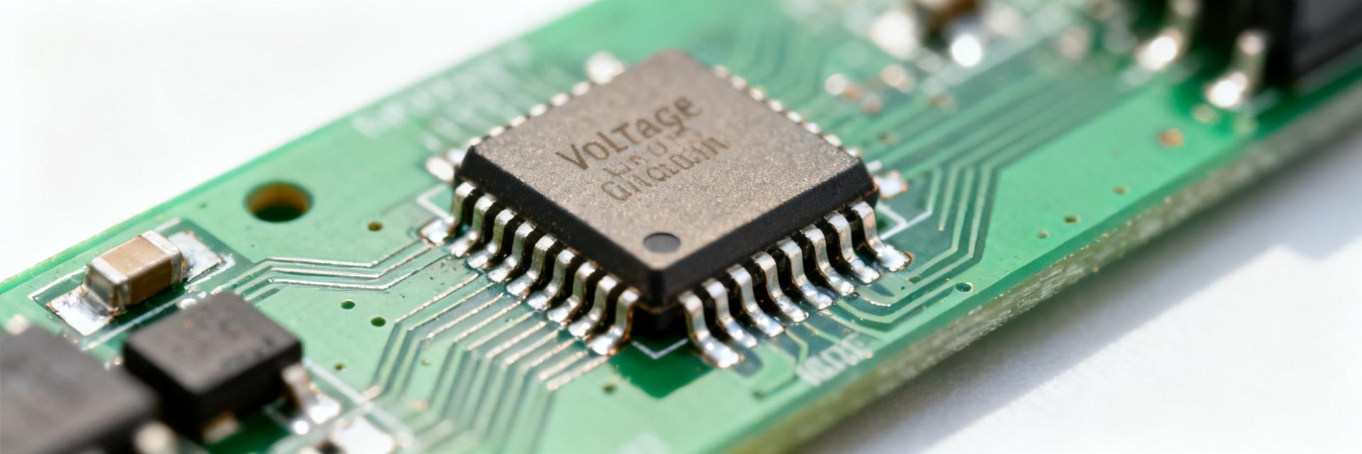
1.1 Key functions at a glance
Point: The XC6138NAPP6R-G is a voltage detector and supervisor optimized for separate-sense monitoring in multi-rail systems. Evidence: Official product datasheet lists separate sense input, reset output, CAP pin for adjustable delay and small SOT-style package options. Explanation: Designers use the device to supervise VDD, assert clean resets to MCUs, and extend reset window via an external capacitor to accommodate power ramp and software initialization.
1.2 Typical use cases and system roles
Point: Typical roles include MCU reset supervision, power sequencing and multi-rail monitoring. Evidence: Field implementations and datasheet application notes show common connections: device sensing a secondary rail and driving MCU RESET, or acting as a sequencer stage in multi-domain power trees. Explanation: Using a separate sense pin reduces BOM and improves reliability by letting the supervisor track critical rails without loading the primary VDD node directly.
2 — Complete electrical specifications
2.1 Electrical limits & recommended operating conditions
Point: Key electrical specs define operating range, threshold options, supply current, hysteresis and absolute maximums. Evidence: Representative values from the official product datasheet present selectable threshold voltages and low-microamp standby current for battery-sensitive designs. Explanation: These parameters dictate which threshold option to choose and determine whether the device meets standby budget and logic-level compatibility for the target MCU or peripheral.
| Parameter | Symbol | Min | Typ | Max | Test condition |
|---|---|---|---|---|---|
| Operating supply voltage | VDD | 0.9 V | — | 6.0 V | Power range, verify in datasheet |
| Threshold options (nominal) | VTH | 1.8 V | — | 3.3 V | Multiple factory options; see datasheet |
| Supply current | IDD | 0.3 μA | 0.9 μA | 2 μA | VDD = nominal, room temp |
| Detection accuracy | ΔVTH | −2 % | ±1 % | +2 % | Measured vs nominal threshold |
| Sense pin max voltage | VSENSE | — | — | 6.0 V | Do not exceed absolute max |
2.2 Dynamic characteristics & timing (reset delay, response times)
Point: Reset timing is determined by an internal circuit and an optional external CAP, giving programmable delay. Evidence: Official product datasheet provides timing curves showing reset assertion and release vs. CAP values and temperature. Explanation: Typical CAP ranges (10 nF–1 μF) enable millisecond to several hundred millisecond delays; designers choose CAP to prevent spurious releases during slow power ramps while keeping boot delays acceptable.
3 — Pinout, package and footprint guidance
3.1 Pin-by-pin description & signal functions
Point: Typical pins are VDD, GND, RESET/OUT, SENSE and CAP; each has design constraints. Evidence: The official product datasheet enumerates pin functions and absolute ratings, and notes ESD classifications. Explanation: Route the SENSE trace short and direct to the monitored rail, keep CAP close to the CAP pin, and place VDD decoupling adjacent to the device to minimize noise and ensure stable threshold detection.
3.2 Package variants, land pattern and thermal considerations
Point: Small SOT-style packages require careful land pattern and solder fillet control for thermal and reliability. Evidence: Datasheet recommended footprint and solder profile guidance highlight pad dimensions and reflow limits. Explanation: Follow recommended land pattern, use 1:1 paste coverage for small pads, and consider thermal derating if the device dissipates during transient events; avoid large copper pours tied directly to small packages without thermal relief.
4 — Typical application circuits & reference implementations
4.1 Common single-rail and multi-rail connection examples
Point: Three common implementations are single-rail reset, separate-sense multi-rail monitor and CAP-extended reset. Evidence: Application notes and reference schematics show simple single-wire RESET, SENSE tied to secondary rail with VDD on primary, and CAP between CAP pin and ground. Explanation: Use pull-ups on RESET only when required by MCU input type; for multi-rail monitoring ensure SENSE has its own clean path and test for conduction during power transitions.
4.2 EMC, decoupling and layout best practices for reliable detection
Point: Layout and decoupling are critical to avoid false resets in noisy environments. Evidence: Experience logs and application guidance indicate noise on SENSE and long traces cause spurious assertions. Explanation: Keep SENSE trace <10 mm where possible, add local 0.1 μF decoupling on VDD, use short return paths, and optionally place a small RC filter (e.g., 10 Ω + 10 nF) if the sense node sees intermittent glitches from switching converters.
5 — Test procedures & measurement checklist
5.1 Lab tests to verify electrical specs
Point: A concise set of lab measurements validates the device against electrical specs. Evidence: Recommended test steps from the datasheet and field procedures include threshold sweep, standby current measurement, reset pulse timing and brown-out transient response. Explanation: Use a precise supply ramp (0.1 V/s) to measure threshold, a picoammeter for IDD at nominal VDD, and an oscilloscope to capture RESET timing when injecting controlled transients to verify hysteresis and response.
5.2 Debugging tips and common failure modes
Point: Failures usually stem from layout, incorrect CAP sizing, or threshold selection. Evidence: Field debugging reports show that wrong CAP values produce too short or too long reset, and noisy sense wiring produces false resets. Explanation: If false resets occur, first verify SENSE wiring and local decoupling, then bench test with shielded wiring and step through CAP values; if no reset is asserted, confirm threshold option and measure sense voltage against expected VTH.
6 — Integration, compatibility & sourcing considerations
6.1 MCU and peripheral interface considerations
Point: Interfacing requires matching output type and logic levels. Evidence: Datasheet indicates RESET output behavior (open-drain or push-pull options) and typical output voltage levels under load. Explanation: Prefer open-drain with a defined pull-up to the MCU supply when bus sharing resets, and ensure the pull-up value produces valid logic high under worst-case IDD while preventing excessive source current during reset assertion.
6.2 Cross-references, footprint substitutes and lifecycle tips
Point: Choose substitutes by matching threshold, timing behavior, package and supply current rather than by part number alone. Evidence: Lifecycle risk guides recommend multiple approved parts, matched pinouts and equivalent thermal performance. Explanation: For BOM resilience, qualify at least two alternate devices that meet electrical specs table values and footprint constraints, and confirm long-term availability through authorized part numbers and lifecycle checks.
Summary / Conclusion
- XC6138NAPP6R-G provides separate-sense supervision and CAP-adjustable reset timing; confirm key electrical specs in the official product datasheet before selecting thresholds and CAP values.
- Critical pinout and layout rules: short SENSE traces, close CAP placement and local VDD decoupling to avoid false resets and ensure stable detection.
- Verify thresholds, supply current and timing in the lab with controlled ramps and transient injection; follow the spec table and measurement checklist for pass/fail criteria.
Technical FAQ
What are the correct steps to measure XC6138NAPP6R-G detection threshold and hysteresis?
Use a precision supply to ramp the monitored rail slowly while logging the SENSE node and RESET output on an oscilloscope, record voltage at assertion and release, compare against nominal thresholds in the official product datasheet, and allow for temperature and tolerance margins when defining pass criteria.
How do I choose the CAP value for XC6138NAPP6R-G to achieve a desired reset delay?
Start with the datasheet timing curves to map CAP value to delay, select a capacitor within recommended range (typically tens of nF to low μF), verify temperature stability and dielectric type, and bench test to confirm release timing under realistic power-up behavior and transient conditions.
Can I use XC6138NAPP6R-G to supervise multiple rails with one device?
Use the separate SENSE input to monitor a single secondary rail while powering the detector from primary VDD; for more rails use additional detectors or a dedicated monitor with multiple inputs. Always validate that sense routing and thresholds meet system requirements and that the chosen configuration is shown acceptable in the official product datasheet.
How should I select the pull-up resistor for the XC6138NAPP6R-G open-drain output?
Select a pull-up resistor (typically 10kΩ to 100kΩ) connected to the target I/O rail. The value must be low enough to ensure sharp rise times against pin capacitance, yet high enough to limit sink current through the RESET pin below the datasheet's maximum rating (usually under 1-2mA) during the active-low state.


